- 您现在的位置:买卖IC网 > Sheet目录3876 > PIC18F14K50-I/SS (Microchip Technology)IC PIC MCU FLASH 8KX16 20-SSOP
2010 Microchip Technology Inc.
Preliminary
DS41350E-page 101
PIC18F/LF1XK50
10.0
TIMER0 MODULE
The Timer0 module incorporates the following features:
Software selectable operation as a timer or coun-
ter in both 8-bit or 16-bit modes
Readable and writable registers
Dedicated 8-bit, software programmable
prescaler
Selectable clock source (internal or external)
Edge select for external clock
Interrupt-on-overflow
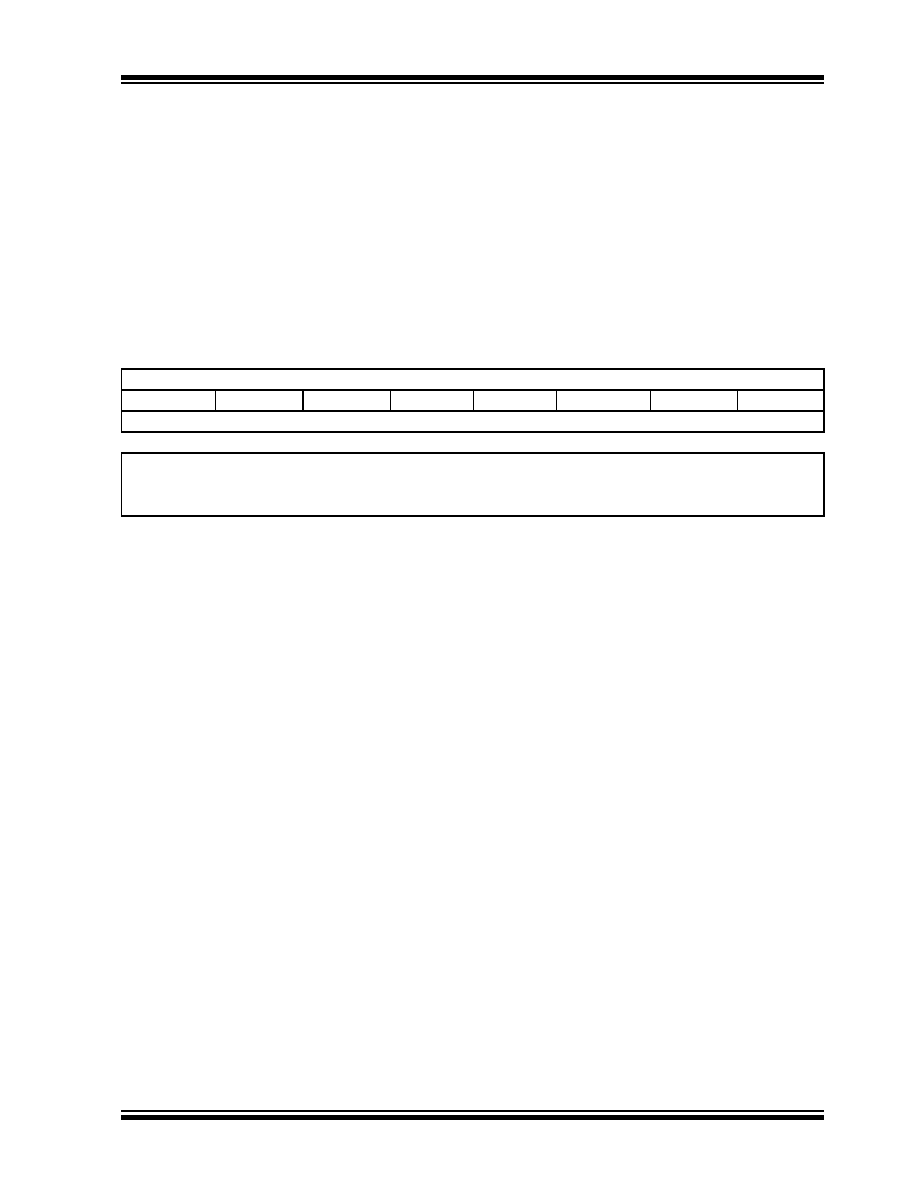
The T0CON register (Register 10-1) controls all
aspects of the module’s operation, including the
prescale selection. It is both readable and writable.
A simplified block diagram of the Timer0 module in 8-bit
mode is shown in Figure 10-1. Figure 10-2 shows a
simplified block diagram of the Timer0 module in 16-bit
mode.
REGISTER 10-1:
T0CON: TIMER0 CONTROL REGISTER
R/W-1
TMR0ON
T08BIT
T0CS
T0SE
PSA
T0PS2
T0PS1
T0PS0
bit 7
bit 0
Legend:
R = Readable bit
W = Writable bit
U = Unimplemented bit, read as ‘0’
-n = Value at POR
‘1’ = Bit is set
‘0’ = Bit is cleared
x = Bit is unknown
bit 7
TMR0ON: Timer0 On/Off Control bit
1
= Enables Timer0
0
= Stops Timer0
bit 6
T08BIT: Timer0 8-bit/16-bit Control bit
1
= Timer0 is configured as an 8-bit timer/counter
0
= Timer0 is configured as a 16-bit timer/counter
bit 5
T0CS: Timer0 Clock Source Select bit
1
= Transition on T0CKI pin
0
= Internal instruction cycle clock (CLKOUT)
bit 4
T0SE: Timer0 Source Edge Select bit
1
= Increment on high-to-low transition on T0CKI pin
0
= Increment on low-to-high transition on T0CKI pin
bit 3
PSA: Timer0 Prescaler Assignment bit
1
= TImer0 prescaler is NOT assigned. Timer0 clock input bypasses prescaler.
0
= Timer0 prescaler is assigned. Timer0 clock input comes from prescaler output.
bit 2-0
T0PS<2:0>: Timer0 Prescaler Select bits
111
= 1:256 prescale value
110
= 1:128 prescale value
101
= 1:64 prescale value
100
= 1:32 prescale value
011
= 1:16 prescale value
010
= 1:8 prescale value
001
= 1:4 prescale value
000
= 1:2 prescale value
发布紧急采购,3分钟左右您将得到回复。
相关PDF资料
PIC24F08KL302-I/ML
IC MCU 16BIT 8KB FLASH 28-QFN
PIC24F08KL302-I/MQ
IC MCU 16BIT 8KB FLASH 28-QFN
PIC16LF627A-I/P
IC MCU FLASH 1KX14 EEPROM 18DIP
PIC18F25K20-I/SO
IC PIC MCU FLASH 16KX16 28SOIC
PIC24F08KL301-I/SO
IC MCU 16BIT 8KB FLASH 20-SOIC
PIC24F04KL101-I/P
IC MCU 16BIT 4KB FLASH 20-PDIP
PIC16LC56A-04/SO
IC MCU OTP 1KX12 18SOIC
PIC16LF74-I/PTG
IC MCU FLASH 4KX14 44TQFP
相关代理商/技术参数
PIC18F14K50T-I/SO
功能描述:8位微控制器 -MCU 16KB Flash 768 RAM15 I/O 10-B ADC USB 2.0
RoHS:否 制造商:Silicon Labs 核心:8051 处理器系列:C8051F39x 数据总线宽度:8 bit 最大时钟频率:50 MHz 程序存储器大小:16 KB 数据 RAM 大小:1 KB 片上 ADC:Yes 工作电源电压:1.8 V to 3.6 V 工作温度范围:- 40 C to + 105 C 封装 / 箱体:QFN-20 安装风格:SMD/SMT
PIC18F14K50T-I/SS
功能描述:8位微控制器 -MCU 16KB Flash 768 RAM15 I/O 10-B ADC USB 2.0
RoHS:否 制造商:Silicon Labs 核心:8051 处理器系列:C8051F39x 数据总线宽度:8 bit 最大时钟频率:50 MHz 程序存储器大小:16 KB 数据 RAM 大小:1 KB 片上 ADC:Yes 工作电源电压:1.8 V to 3.6 V 工作温度范围:- 40 C to + 105 C 封装 / 箱体:QFN-20 安装风格:SMD/SMT
PIC18F2220-E/SO
功能描述:8位微控制器 -MCU 4KB 512 RAM 25 I/O RoHS:否 制造商:Silicon Labs 核心:8051 处理器系列:C8051F39x 数据总线宽度:8 bit 最大时钟频率:50 MHz 程序存储器大小:16 KB 数据 RAM 大小:1 KB 片上 ADC:Yes 工作电源电压:1.8 V to 3.6 V 工作温度范围:- 40 C to + 105 C 封装 / 箱体:QFN-20 安装风格:SMD/SMT
PIC18F2220-E/SP
功能描述:8位微控制器 -MCU 4KB 512 RAM 25 I/O RoHS:否 制造商:Silicon Labs 核心:8051 处理器系列:C8051F39x 数据总线宽度:8 bit 最大时钟频率:50 MHz 程序存储器大小:16 KB 数据 RAM 大小:1 KB 片上 ADC:Yes 工作电源电压:1.8 V to 3.6 V 工作温度范围:- 40 C to + 105 C 封装 / 箱体:QFN-20 安装风格:SMD/SMT
PIC18F2220-I/SO
功能描述:8位微控制器 -MCU 4KB 512 RAM 25 I/O RoHS:否 制造商:Silicon Labs 核心:8051 处理器系列:C8051F39x 数据总线宽度:8 bit 最大时钟频率:50 MHz 程序存储器大小:16 KB 数据 RAM 大小:1 KB 片上 ADC:Yes 工作电源电压:1.8 V to 3.6 V 工作温度范围:- 40 C to + 105 C 封装 / 箱体:QFN-20 安装风格:SMD/SMT
PIC18F2220-I/SO
制造商:Microchip Technology Inc 功能描述:IC 8BIT FLASH MCU 18F2220 SOIC28
PIC18F2220-I/SOC03
制造商:Microchip Technology Inc 功能描述:
PIC18F2220-I/SP
功能描述:8位微控制器 -MCU 4KB 512 RAM 25 I/O RoHS:否 制造商:Silicon Labs 核心:8051 处理器系列:C8051F39x 数据总线宽度:8 bit 最大时钟频率:50 MHz 程序存储器大小:16 KB 数据 RAM 大小:1 KB 片上 ADC:Yes 工作电源电压:1.8 V to 3.6 V 工作温度范围:- 40 C to + 105 C 封装 / 箱体:QFN-20 安装风格:SMD/SMT